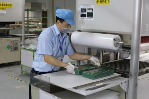
PCB assembly/SMT
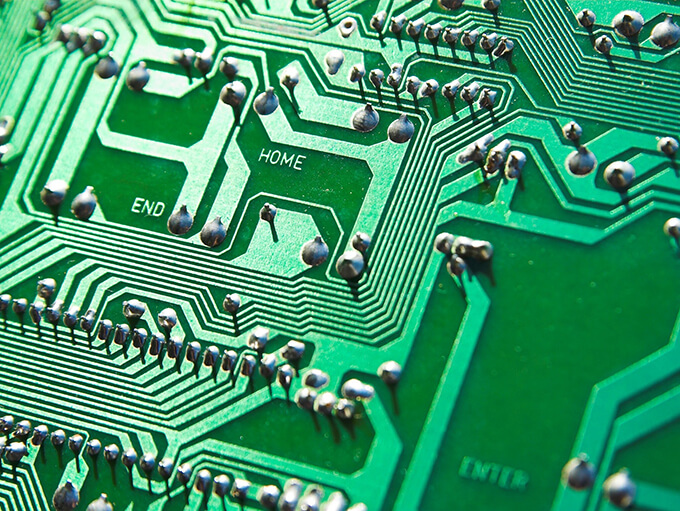 PCB Manufacturing
 Components Sourcing
 PCB design
PCB deformation acceptance criteria
What is the standard for PCB deformation -: Refer to IPC-A-600G No. 2.11 for PCB deformation standard. Flatness standard: For printed boards with surface mount components (such as SMT mounting), the standard for warp and bending is no more than 0.75%, other types of boards are no more than 1.5%. The test method refers to IPC-TM-650 2.4.22.
 Is there a standard for PCB deformation? How to measure it? How is the V-CUT standard stipulated? -: Some companies set it like this: diagonal (or long side) * 0.7% + panel thickness, so the upper limit is set to diagonal (long side) * 0 , 5% + plate thickness (standard center value) of course, some products are also set at 0.5% or 0.4%, mainly according to the product characteristics and thickness. If it is a thin plate, the deformation is often greater. When measuring …
Look for all substrate types and deformation standards for PCB board -: If it is fr4 material: * board thickness has little effect * is that the stress of the pressing station during the PCB manufacturing process is not released, which may cause the carton to deform * the multilayer carton pressing process, The positioning of the adhesive sheet (film) is out of place, causing the smt to pass through the oven. The upper and lower oven temperature of the smt station is abnormal. If it is an aluminum support (one-sided): * it will be a normal phenomenon that the plate is too high to dent the oven. , That is, the aluminum-based material is not good, and the material with poor temperature resistance will be.
How to judge the PCB flatness acceptance standard?
The IPC secondary standard is 7.5 per thousandth of the total diagonal length of the board, which is used as a criterion for judging the warp of the board. That is, put the PCB on the flat surface and press one of your fingers. Angle, the ratio between the height of the inclined end and the diagonal length of the pcb.
How to measure the deformation of the PCB?
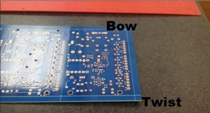
The deformation of the PCB includes arc and twist. The measurement methods and calculation formulas of the two are different. This is usually not the case with beginners and those who have been making printed circuit boards for several years. Understand the problem. The bow also bends. If the deformation of the circuit is this case, the measurement method is to lay it flat on the marble and the four corners of the circuit are on the ground. The measure is …
How to Measure PCB Deformation
Place the PCB to be measured on the marble worktop and use a pad gauge (wobbly type) to measure. If you remember correctly, the standard calculation is:
What are the inspection standards for PCB board appearance?
1. Packing: Colorless air ball bag vacuum packing, with desiccant inside, well packed 2. Screen printing: The screen printing of the characters and symbols on the PCB surface should be clear, obvious, and the color meets the requirements, There are no repeated prints, missing prints, multiple prints, position deviations, incorrect prints. 3. Board Edge Surface: Check for stains, debris, holes, tin slag on the PCB surface …
How to measure the deformation of the PCB board?
There are three methods I know of: 1. Use the marble platform to test, which is also a method used by many manufacturers. The sound produced by the space between the marble shelves will be leveled by the feel of the hand. 2. The laser test method, the accuracy can be 0.1mm3, the optical detection method, using the principle of light interference, deformation and distortion test, etc., the accuracy can reach 0.1 mil, the our company is the agent of this equipment, called akrometrix, which is used for mass production and shipment inspection, or for laboratory simulation of reflow soldering for analysis.
PCB Board Inspection Standards
Original Publisher: dlhss1 Printed Circuit Inspection Standard 1. Scope is applicable to inbound inspection of mobile phone HDI circuits. 2. The sampling plan is based on GB2828.1-2003, general inspection level II The inspection is performed at level 3. The inspection is based on the technical specifications of the raw materials and the inspection samples. 4. The qualified quality level is based on the AQL value: Class A = 0.01, Class B = 0.65, Class C = 2.5.5 …
ipc-a-610d how to calculate the deformation of the board: The so-called deformation of the PCB is used to control the deformation of the PCB. Deformation = HL≤0.005H is the height of the deform
The calculation formula for PCB board deformation value:
PCB deformation includes arc and twist. The measurement methods and calculation formulas of the two are different. This is usually not understood by beginners and those who have been making printed circuit boards for several years. The problem with bowing is bending. If the twist of the circuit is this case, the measurement method is to flatten it on the marble, and the four corners of the circuit are on the ground, and the height of the central arc is measured; the calculation method is: Deformation Degree = arc height / PCB long side length * 100% The distortion measurement method consists in touching the ground at the three corners and measuring the height of the inclined angle from the ground; the calculation method is: warpage = the height of a single corner / (PCB diagonal length * 2) * 100%; If the PCB has both curvature and torsion defects, the more serious one will prevail. If you don’t understand, please refer to the relevant chapters of IPC-650.
What is the formula for calculating the deformation value of the “pcb” board?
Deformation = deformation height of a single corner / (diagonal length of the PCB * 2) * 100% Detailed introduction to deformation The deformation is a plastic part It is not formed according to the designed shape, but the surface is distorted. The deformation of the plastic part is caused by the uneven shrinkage of the formed plastic part. If the entire plastic part has a uniform shrinkage rate, the plastic part will not deform, only. ..
What is the standard for PCB deformation?
Refer to IPC-A-600G No. 2.11 for PCB deformation standard. Flatness standard: For printed boards with surface mount components (such as SMT mounting), the standard for warp and bending is no more than 0.75%, other types of boards are no more than 1.5%. The test method refers to IPC-TM-650 2.4.22.
PCB board deformation formula questions?
1. Strain = (maximum single angle strain height ÷ substrate diagonal length) * 100% 2. The diagonal length is usually calculated by the Pythagorean theorem, such as: a, b is the length and width of the support, C is the diagonal length, therefore: C² = a² + b²3, the deformation standard generally accepted in the IPC industry is 0.75%, unless the customer has special needs; the above.If you are not clear, you can ask me again. Thanks and I hope to adopt it.
How to Measure PCB Deformation
Place the PCB to be measured on the marble worktop and use a pad gauge (wobbly type) to measure. If you remember correctly, the standard calculation is:
Is there a standard for PCB deformation? How to measure it? How is the V-CUT standard stipulated?
Some companies set it like this: diagonal (or long side) * 0.7% + panel thickness, so the upper limit is set to diagonal (long side) * 0 , 5% + plate thickness (standard center value) of course, some products are also set at 0.5% or 0.4%, mainly according to the product characteristics and thickness. If it is a thin plate, the deformation is often greater. When measuring …
The Calculation Method for PCB Cutting Materials “ Who knows that ‘that big brother can help the little brother’? Thanks in advance! Device pins are irregular, assembly / installation is difficult; IPC-6012, SMB-SMT printed circuit boards have a maximum deformation or distortion of 0.75%, and the deformation of other boards generally does not exceed 1.5%; the deformation allowed by the electronic assembly factory (double-sided / multilayer) usually 0.70 — 0.75 …
ipc-a-610d how to calculate the deformation of the board: The so-called deformation of the PCB is used to control the deformation of the PCB. Deformation = HL≤0.005H is the height of the deformation (excluding the thickness of the panel) L is the length of the deformed panel Put it on the glass platform and use the vernier caliper and pin gauge to test the inspection of standard quality of double-sided multilayer PCB
Find the formula to calculate the bending stiffness of the plastic plate -: In engineering applications, you can directly consult the table when using the stiffness calculation, but if the known conditions are insufficient, you can use the following formula to calculate : w ” = -M (x) / EI where: w-deflection; M (x) -bending moment of the section; EI-is the required stiffness, which indicates the ability of the element to resist deformation; w can be measured through experiments and the calculation formula for the bending moment M (x) can be obtained. Go back and check the table !! Generally, there is no need for calculations.
In the automated surface mount line, if the circuit board is not flat, it will cause inaccurate positioning, components cannot be inserted or mounted on the holes and surface mount pads of the board, and even the automatic insertion machine will be damaged. The circuit board on which the components are installed is bent after soldering, and the component feet are difficult to cut neatly. The board cannot be installed on the chassis or the socket inside the machine, so it is also very annoying for the assembly plant to encounter the board warping. The current surface mount technology is developing in the direction of high precision, high speed, and intelligence, which puts forward higher flatness requirements for PCB boards that are home to various components.
In the IPC standard, it is specifically pointed out that the maximum allowable deformation of PCB boards with surface mount devices is 0.75%, and the maximum allowable deformation of PCB boards without surface mounting is 1.5%. In fact, in order to meet the requirements of high-precision and high-speed placement, some electronic assembly manufacturers have stricter requirements on the amount of deformation.
The PCB board is composed of copper foil, resin, glass cloth and other materials. The physical and chemical properties of each material are different, and thermal stress will inevitably occur after being pressed together, which will cause deformation. At the same time, in the PCB processing process, it will go through various processes such as high temperature, mechanical cutting, wet treatment, etc., which will also have an important impact on the deformation of the board. In short, the reasons for the deformation of the PCB can be complex and diverse. How to reduce or eliminate the material characteristics Distortion or deformation caused by processing has become one of the most complicated problems faced by PCB manufacturers.
2. Analysis of the causes of deformation
The deformation of PCB board needs to be studied from several aspects such as material, structure, pattern distribution, processing process, etc. This article will analyze and explain various reasons and improvement methods that may occur.
The uneven copper surface area on the circuit board will worsen the bending and warping of the board.
Generally, a large area of copper foil is designed on the circuit board for grounding purposes. Sometimes there is also a large area of copper foil designed on the Vcc layer. When these large area copper foils cannot be evenly distributed on the same circuit board When it is installed, it will cause uneven heat absorption and heat dissipation. Of course, the circuit board will also expand and contract. If the expansion and contraction cannot be done at the same time, it will cause different stress and deformation. At this time, if the temperature of the board has reached At the upper limit of the Tg value, the board will begin to soften, causing permanent deformation.
The connection points (vias, vias) of each layer on the circuit board will limit the expansion and contraction of the board
Today’s circuit boards are mostly multi-layer boards, and there will be rivet-like connection points (vias) between the layers. The connection points are divided into through holes, blind holes and buried holes. Where there are connection points, the board will be restricted. The effect of expansion and contraction will also indirectly cause plate bending and plate warping.
The weight of the circuit board itself will cause the board to dent and deform
Generally, the reflow furnace uses a chain to drive the circuit board forward in the reflow furnace, that is, the two sides of the board are used as fulcrums to support the entire board. If there are heavy parts on the board, or the size of the board is too large, It will show a depression in the middle due to the amount of seed, causing the plate to bend.
The depth of the V-Cut and the connecting strip will affect the deformation of the jigsaw
Basically, V-Cut is the culprit that destroys the structure of the board, because V-Cut cuts grooves in the original large sheet, so the V-Cut is prone to deformation.

2.1 Analysis of the influence of pressing materials, structures, and graphics on plate deformation
The PCB board is formed by pressing the core board, the prepreg and the outer copper foil. The core board and the copper foil are deformed by heat when they are pressed together. The amount of deformation depends on the coefficient of thermal expansion (CTE) of the two materials.
The coefficient of thermal expansion (CTE) of copper foil is about
The Z-direction CTE of the ordinary FR-4 substrate at the Tg point is;
Above the TG point is (250~350)X10-6, and the X-direction CTE is generally similar to copper foil due to the presence of glass cloth.
Notes on TG point:
When the temperature of a high Tg printed board rises to a certain area, the substrate will change from the “glass state” to the “rubber state”. The temperature at this time is called the glass transition temperature (Tg) of the board. That is, Tg is the highest temperature (°C) at which the base material maintains rigidity. That is to say, ordinary PCB substrate materials not only produce softening, deformation, melting and other phenomena at high temperatures, but also exhibit a sharp decline in mechanical and electrical properties.
Generally, the Tg of the board is above 130 degrees, the high Tg is generally greater than 170 degrees, and the medium Tg is about greater than 150 degrees.
Usually PCB printed boards with Tg≥170℃ are called high Tg printed boards.
As the Tg of the substrate is increased, the heat resistance, moisture resistance, chemical resistance, stability and other characteristics of the printed board will be improved and improved. The higher the TG value, the better the temperature resistance of the board. Especially in the lead-free process, high Tg applications are more common.
High Tg refers to high heat resistance. With the rapid development of the electronics industry, especially the electronic products represented by computers, the development of high functionality and high multilayers requires higher heat resistance of PCB substrate materials as an important guarantee. The emergence and development of high-density mounting technologies represented by SMT and CMT have made PCBs more and more inseparable from the support of high heat resistance of substrates in terms of small aperture, fine wiring, and thinning.
Therefore, the difference between general FR-4 and high Tg FR-4 is the mechanical strength, dimensional stability, adhesion, water absorption, and thermal decomposition of the material in the hot state, especially when heated after moisture absorption. There are differences in various conditions such as thermal expansion, and high Tg products are obviously better than ordinary PCB substrate materials.
Among them, the expansion of the core board with the inner layer pattern is different due to the difference between the pattern distribution and the thickness of the core board or the material characteristics. When the pattern distribution is different from the thickness of the core board or the material characteristics, it will be different. Will be deformed. When the PCB laminate structure has asymmetry or uneven pattern distribution, the CTE of different core boards will vary greatly, which will cause deformation during the lamination process. The deformation mechanism can be explained by the following principles.
2.2 Deformation caused during PCB processing
The reason for the deformation of PCB board processing is very complicated and can be divided into two kinds of stress: thermal stress and mechanical stress. Among them, the thermal stress is mainly generated during the pressing process, and the mechanical stress is mainly generated during the stacking, handling and baking of the plates. The following is a brief discussion in the order of the process.
Incoming copper clad laminate: The copper clad laminates are all double-sided, with symmetrical structure and no graphics. The CTE of copper foil and glass cloth is almost the same, so there is almost no deformation caused by the difference in CTE during the pressing process. However, the size of the copper clad laminate press is large, and the temperature difference in different areas of the hot plate will cause slight differences in the resin curing speed and degree in different areas during the pressing process. At the same time, the dynamic viscosity at different heating rates is also quite different, so it will also produce Local stress due to differences in curing process. Generally, this kind of stress will maintain balance after pressing, but will gradually release and deform during future processing.
Pressing: The PCB pressing process is the main process that generates thermal stress. The deformation due to different materials or structures is shown in the analysis in the previous section. Similar to the pressing of copper clad laminates, local stresses caused by differences in the curing process will also occur. PCB boards have more thermal stress than copper clad laminates due to thicker thickness, diverse pattern distribution, and more prepregs. The stress in the PCB board is released during subsequent drilling, shape, or grilling processes, causing the board to deform.
Baking process of solder mask, characters, etc.: As solder mask inks cannot be stacked on each other when they are cured, PCB boards will be placed in a rack for curing. The solder mask temperature is about 150°C, which just exceeds the Tg point of medium and low Tg materials, Tg The resin above the point is highly elastic, and the plate is easily deformed under the action of its own weight or the strong wind of the oven.
Hot-air solder leveling: The temperature
of the tin furnace is 225℃~265℃, and the time is 3S-6S when the ordinary board hot-air solder is leveled. The hot air temperature is 280℃~300℃. When the solder is leveled, the board is put into the tin furnace from room temperature, and the post-treatment water washing at room temperature will be carried out within two minutes after being out of the furnace. The entire hot-air solder leveling process is a sudden heating and cooling process. Due to the different materials of the circuit board and the uneven structure, thermal stress will inevitably appear during the cooling and heating process, leading to microscopic strain and overall deformation and warping area.
Storage: The storage of PCB boards at the stage of semi-finished products is generally firmly inserted in the shelf, and the tightness of the shelf is not adjusted properly, or the stacking of the boards during the storage process will cause mechanical deformation of the boards. Especially for thin plates below 2.0mm, the impact is more serious.
In addition to the above factors, there are many factors that affect PCB deformation. 3. Improvement measures
So how can we prevent the board from bending and warping when the board passes through the reflow furnace?
1. Reduce the effect of temperature on the stress of the board
Since “temperature” is the main source of board stress, as long as the temperature of the reflow furnace is lowered or the rate of heating and cooling of the board in the reflow furnace is slowed, the occurrence of plate bending and warpage can be greatly reduced. But there may be other side effects.
2. Using high Tg sheet
Tg is the glass transition temperature, that is, the temperature at which the material changes from the glass state to the rubber state. The lower the Tg value of the material, the faster the board starts to soften after entering the reflow oven, and the time it takes to become soft rubber state It will also become longer, and the deformation of the board will of course be more serious. The use of a higher Tg sheet can increase its ability to withstand stress and deformation, but the price of the material is relatively high.
3. Increase the thickness of the circuit board
In order to achieve the purpose of lighter and thinner for many electronic products, the thickness of the board has left 1.0mm, 0.8mm, or even 0.6mm. Such a thickness must keep the board from deforming after the reflow furnace, which is really difficult. It is recommended that if there is no requirement for lightness and thinness, the thickness of the board should be 1.6mm, which can greatly reduce the risk of bending and deformation of the board.
4. Reduce the size of the circuit board and reduce the number of puzzles
Since most of the reflow furnaces use chains to drive the circuit board forward, the larger the size of the circuit board will be due to its own weight, dent and deformation in the reflow furnace, so try to put the long side of the circuit board as the edge of the board. On the chain of the reflow furnace, the depression and deformation caused by the weight of the circuit board can be reduced. The reduction in the number of panels is also based on this reason. That is to say, when passing the furnace, try to use the narrow edge to pass the furnace direction as far as possible. The amount of depression deformation.
5. Used furnace tray fixture
If the above methods are difficult to achieve, the last is to use a reflow carrier/template to reduce the amount of deformation. The reason why the reflow carrier/template can reduce the bending of the plate is because it is hoped whether it is thermal expansion or cold contraction. The tray can hold the circuit board and wait until the temperature of the circuit board is lower than the Tg value and start to harden again, and can also maintain the size of the garden.
If the single-layer pallet cannot reduce the deformation of the circuit board, a cover must be added to clamp the circuit board with the upper and lower pallets. This can greatly reduce the problem of circuit board deformation through the reflow furnace. However, this furnace tray is quite expensive, and manual labor is required to place and recycle the trays.
6. Use real connections and stamp holes instead of V-Cut sub-boards
Since V-Cut will destroy the structural strength of the panel between the circuit boards, try not to use the V-Cut sub-board or reduce the depth of the V-Cut.
Optimization in PCB production engineering:
The deformation defect rate of low Tg materials is higher than that of high Tg materials. The high Tg materials listed in the above table are all filler-shaped materials, and the CTE is less than that of low Tg materials. At the same time, the baking temperature is up to 150°C during the processing after pressing. The impact on low Tg materials will definitely be greater than that on medium and high Tg materials.
Engineering Design Research
Engineering design should try to avoid structural asymmetry, material asymmetry, and graphic asymmetry design to reduce deformation. At the same time, it was found in the research process that the core plate directly laminated structure is easier to deform than the copper foil laminated structure. Table 2 shows Test results of two structural panels.
In engineering design, the frame form of the jigsaw panel also has a greater impact on the deformation. Generally, PCB factories will have a continuous large copper frame and a non-continuous copper dot or copper block frame, and there are also different differences.
3.3 Compression study
The effect of pressing on deformation is very important, and the generation of stress can be effectively reduced through reasonable parameter settings, press selection and stacking methods. For general panels with symmetrical structures, it is generally necessary to pay attention to symmetrical stacking during pressing, and symmetrical placement of auxiliary tools such as tool panels and cushioning materials. At the same time, choosing the hot and cold integrated press to press is also obviously helpful to reduce the thermal stress. The reason is that the cold and hot split press transfers the plate to the cold press at high temperature (above GT temperature), and the material loses pressure above the Tg point. Rapid cooling will lead to rapid release of thermal stress and deformation, while the integrated cold and heat press can cool down the final stage of hot pressing to prevent the plate from losing pressure at high temperatures.
At the same time, for the special needs of customers, it is inevitable that there will be some plates with asymmetric materials or structures. At this time, the deformation caused by the different CTEs analyzed in the previous article will be very obvious. For this problem, we can try to use asymmetric The principle is to use the asymmetrical placement of the buffer material to achieve different heating speeds on both sides of the PCB, which affects the expansion and contraction of different CTE core cypresses during the heating and cooling stages to solve the problem of inconsistent deformation. Table 4 is the test result on a certain structural asymmetric plate of our company.
Through the asymmetric stacking method, and adding a post-curing process after pressing, and leveling before shipment, this board finally meets the customer’s 2.0mm requirements.
3.4 Other production processes
In the PCB production process, in addition to pressing, there are several high-temperature treatment processes for solder mask, characterization and hot air leveling. Among them, the highest temperature of the solder mask and the baking board after the character is 150 ℃. As mentioned above, this temperature is in the ordinary Tg material. Above the Tg point, the material is in a highly elastic state and is easily deformed under external force. Therefore, avoid stacking the plates to prevent the lower plate from being bent when drying the plates. At the same time, ensure that the plate direction is parallel to the blowing direction when the plates are dried. During the hot air leveling process, it is necessary to ensure that the plate is placed in the tin furnace for cooling for more than 30 seconds to avoid the cold water washing of the post-treatment at high temperature causing sudden cold deformation.
In addition to the production process, the storage of PCB boards at each station also has a certain impact on the deformation. In some manufacturers, due to the large number of products to be produced and the small space, multiple boards are stacked together for storage, which will also cause the board The parts are deformed by external force, and because the PCB board also has a certain degree of plasticity, these deformations will not be 100% restored in the subsequent leveling process.
3.5 Leveling before shipment
Most PCB manufacturers will have a leveling process before shipment. This is because the deformation of the board caused by heat or mechanical force will inevitably occur during the processing. It can be leveled by mechanical leveling or thermal baking before shipment. Be effectively improved. Affected by the heat resistance of the solder mask and the surface coating layer, the general baking temperature is below 140℃~150℃, which just exceeds the Tg temperature of ordinary materials. This has great benefits for the leveling of ordinary boards, but for high Tg materials The leveling effect is not so obvious, so the temperature of the baking sheet can be appropriately increased on the high Tg boards with serious board warpage, but the quality of the ink and coating layer is mainly required. At the same time, the method of weighting during baking and increasing the cooling time with the furnace also has a certain effect on the deformation. Table 5 shows the test results of the leveling effect of different
weights and furnace cooling times on the plate, which can be seen from the increase in weight. And extending the cooling time of the furnace have obvious effects on the leveling of deformation.