 PCB assembly/SMT
 PCB Manufacturing
 Components Sourcing
 PCB design
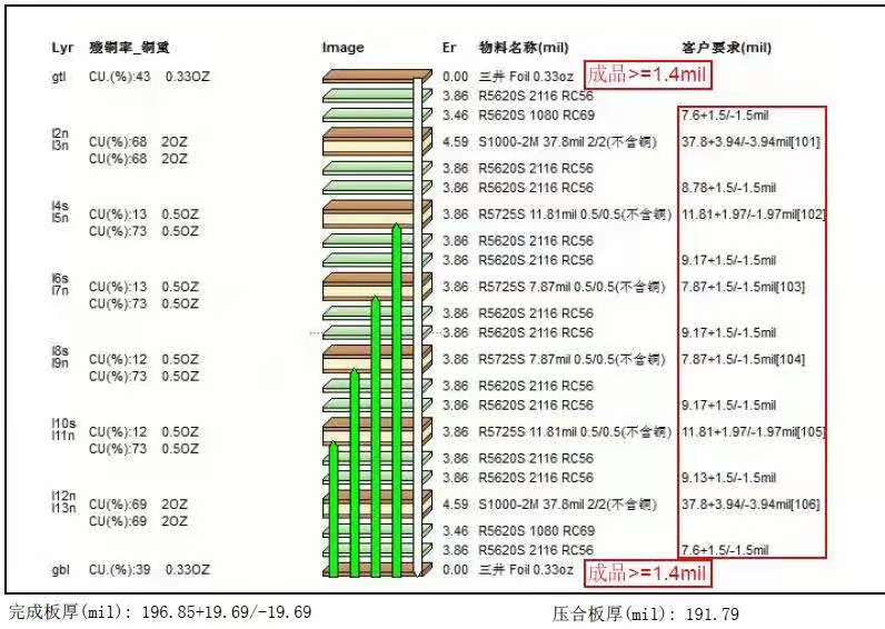
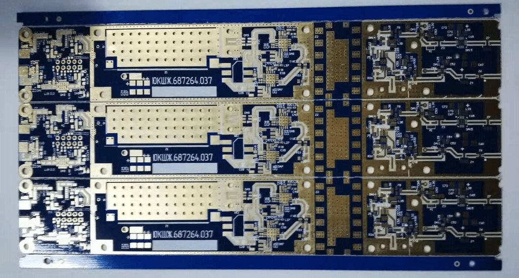
14-layer back drill plate, 5mm thickness, Panasonic plate R5620+S1000-2M lamination PCB
HDI and other special parameter PCB project
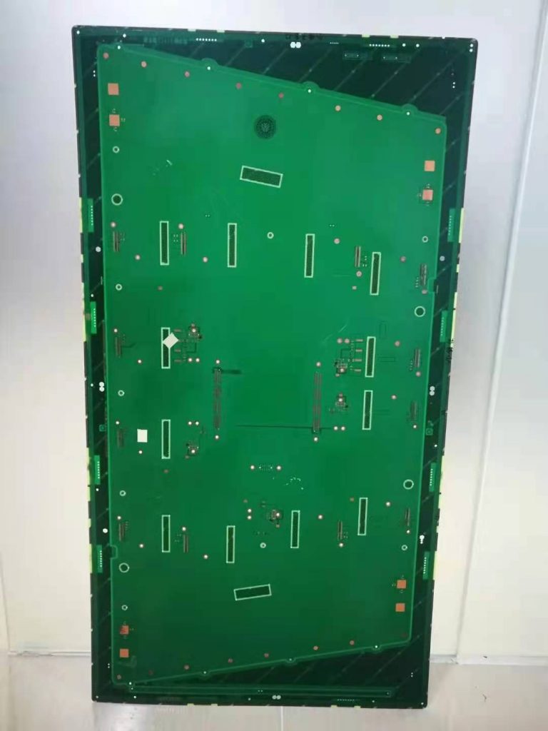
10-layer interconnection HDI board, minimum line width 1.5mil
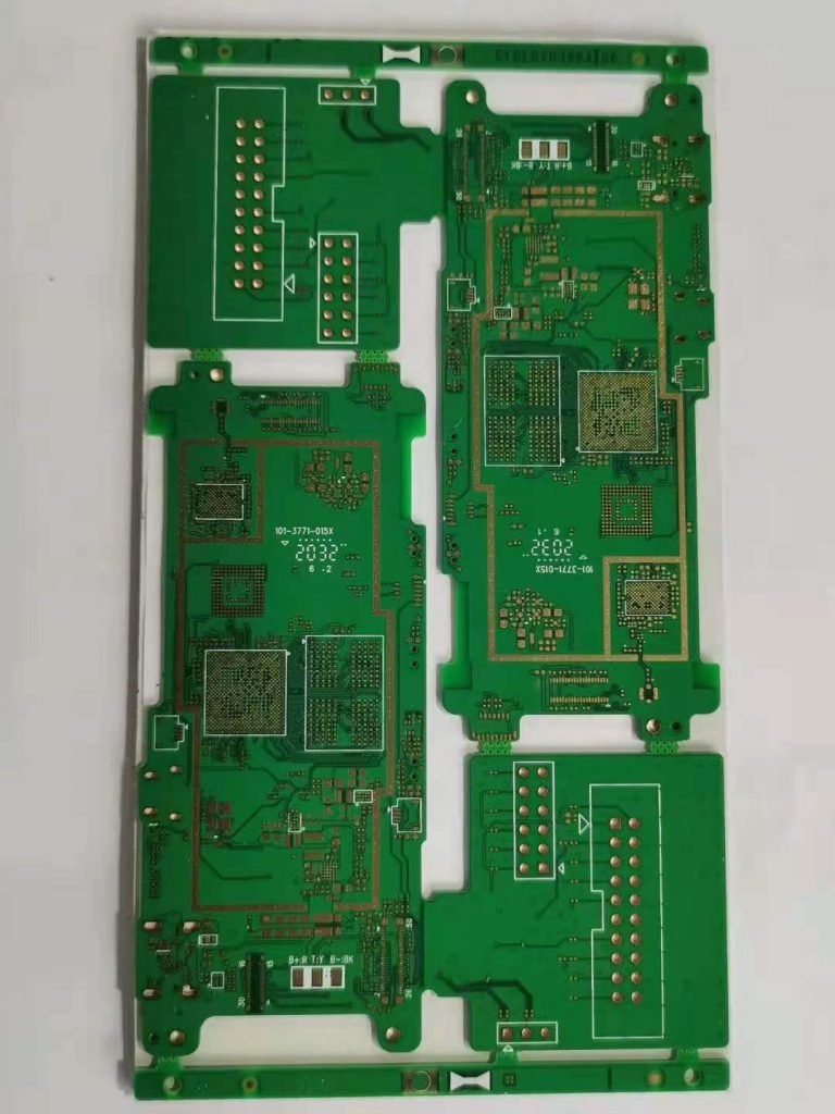
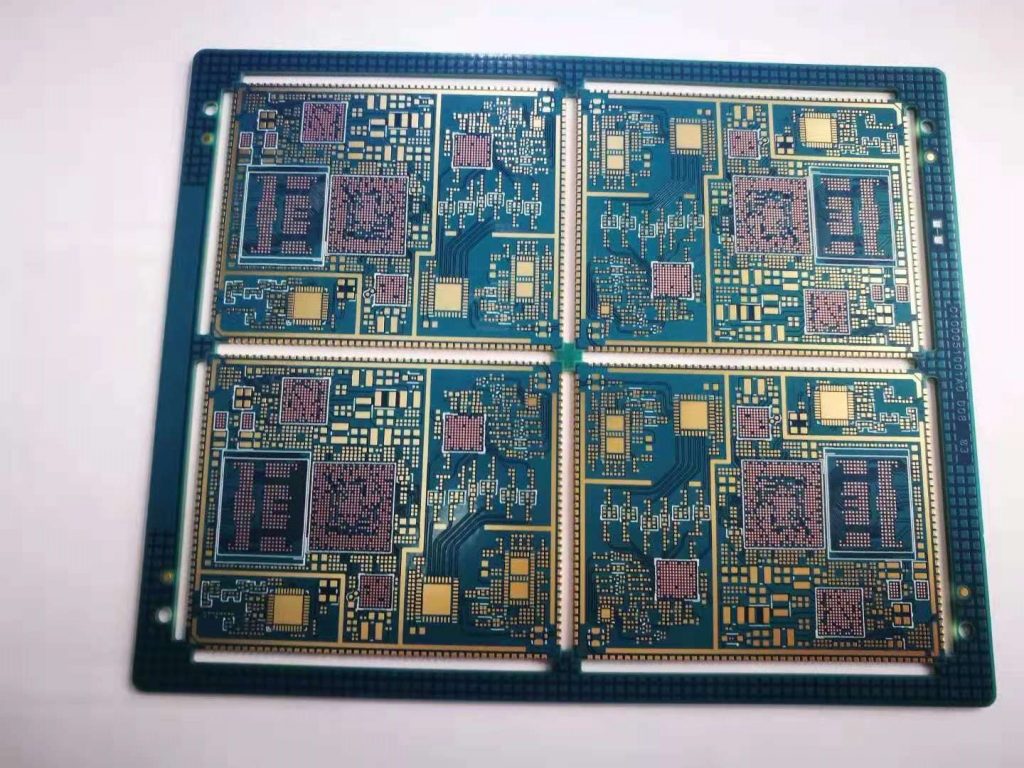
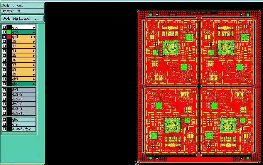
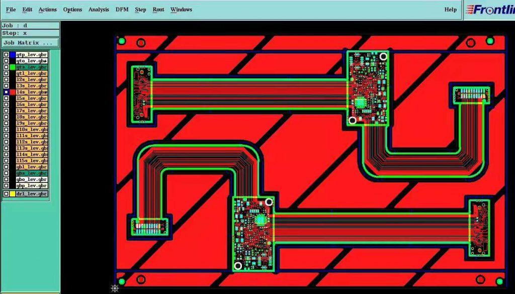
10-layer board, size 1100*430MM,over size PCB board
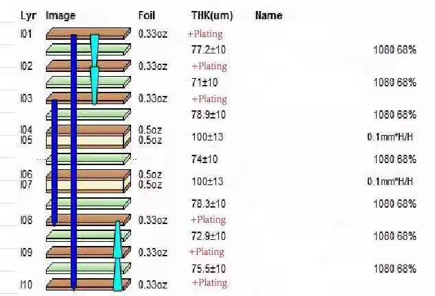
10-layer second-order HDI board, 2+4+2 structure
Led PCB, transparent crystal film screen board. The crystal film is used as the base, and the conductive silver paste circuit is etched on the surface. Crimping forming of external adhesive film
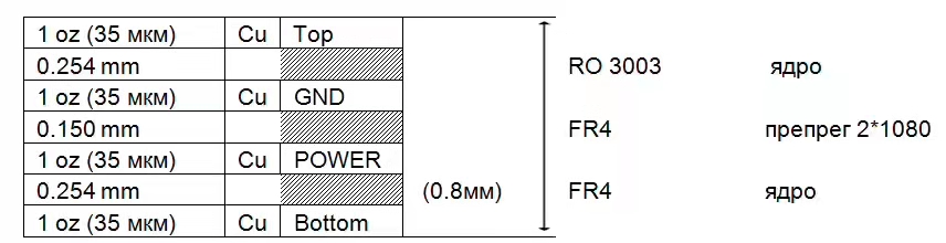
Rogers 3003+FR4 Lamination PCB board
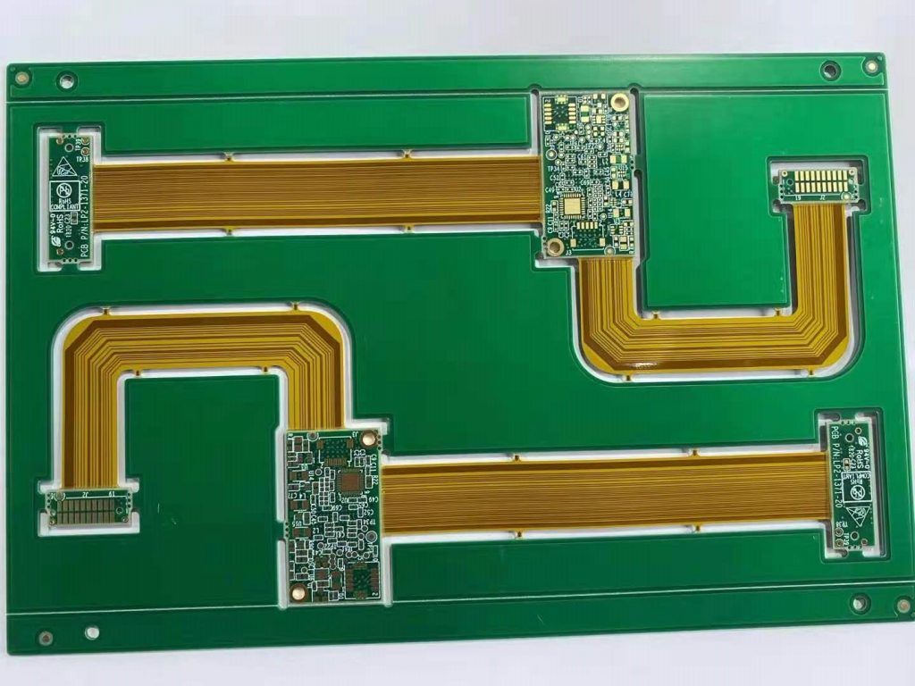
16-layer rigid-flex board, EM827 board, HDI rigid-flex board
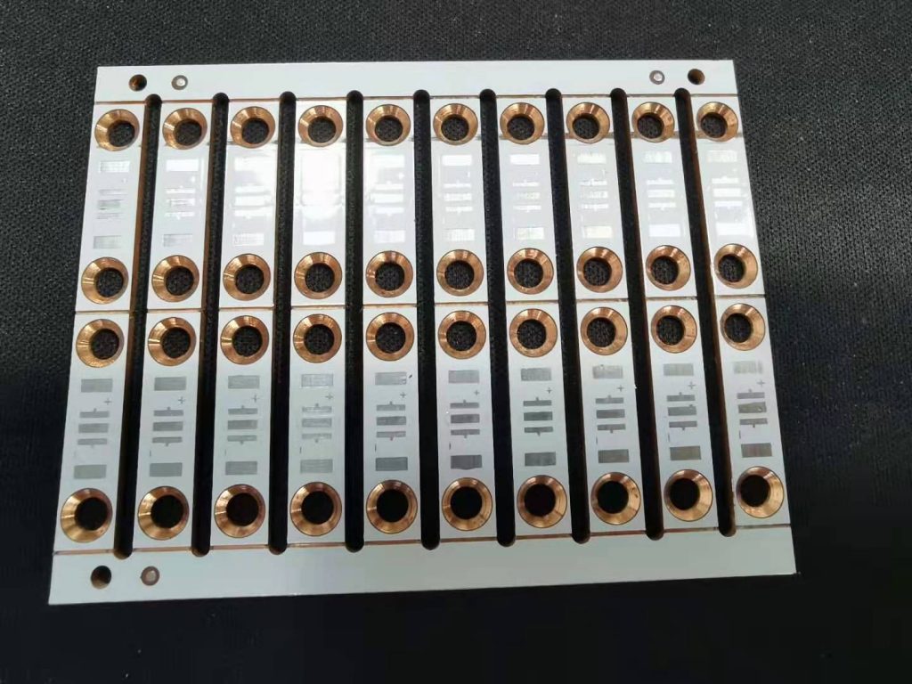
Copper substrate, thermoelectric separation. Horn cone drill hole