 PCB assembly/SMT
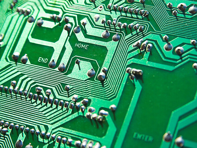 PCB Manufacturing
 Components Sourcing
 PCB design
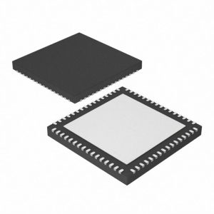
The package quad flat non-leaded package, abbreviated as QFN, is a lead-free package with peripheral terminal pads and a chip pad for mechanical and thermal integrity exposure.
The package can be square or rectangular. The four sides of the package are equipped with electrode contacts. Because there are no leads, the mounting area is smaller than QFP and the height is lower than QFP. There are two kinds of materials: ceramic and plastic. When there is an LCC mark, it is basically ceramic QFN. The electrode contact center distance is 1.27mm. Plastic QFN is a low-cost package of glass epoxy printed substrate substrate. In addition to 1.27mm, there are two types of electrode contact center distance: 0.65mm and 0.5mm. This kind of package is also called plastic LCC, PCLC, P-LCC, etc.
After we complete the PCBA, QC will check the overall soldering quality. For soldering, repair the components that are not good enough for soldering. Or test the NG PCBA during FCT, if it is badly soldered, it will be removed and re-soldered manually.
QFN package advantages and disadvantages
In recent years, QFN package (Quad Flat No-lead, quad flat no-lead package) due to its good electrical and thermal properties, small size, light weight, its application is growing rapidly. The QFN package with a miniature lead frame is called an MLF package (Micro Lead Frame). The QFN package is somewhat similar to the CSP (Chip Size Package), but there is no solder ball on the bottom of the component.
Advantages:
QFN package (quad flat no-lead package) has good electrical and thermal performance, small size, light weight, and its application is growing rapidly; development cost is low, currently many design houses use QFN/DFN as new product development; QFN package The excellent thermal performance is mainly due to the large-area heat dissipation pad at the bottom of the package. In order to effectively conduct heat from the chip to the PCB, the bottom of the PCB must be designed with corresponding heat dissipation pads, heat dissipation vias, and heat dissipation soldering. The pad provides a reliable soldering area, and the via provides a heat dissipation path; because the QFN package does not have gull-wing leads like the traditional SOIC and TSOP packages, the conductive path between the internal pin and the pad is short, the self-inductance and the package The wiring resistance in the body is very low, so it can provide excellent electrical performance; in addition, it also provides excellent heat dissipation performance through the exposed lead frame pad, which has a direct heat dissipation channel to release the heat in the package. Usually the heat dissipation pad is directly soldered on the circuit board, and the heat dissipation vias in the PCB help to diffuse the excess power consumption into the copper ground plane, thereby absorbing the excess heat. The QFN package does not need to lead out pins from both sides, so the electrical performance is better than traditional packages such as SO, where multiple pins must be drawn from the side of the leaded package.
QFN has a very outstanding feature, that is, the QFN package and the ultra-thin small outline package (TSSOP) have the same outer lead configuration, but its size is 62% smaller than that of the TSSOP. According to the QFN modeling data, its thermal performance is 55% higher than the TSSOP package, and the electrical performance (inductance and capacitance) is 60% and 30% higher than the TSSOP package, respectively.
QFN package due to its small size, light weight, coupled with outstanding electrical and thermal properties, this package is particularly suitable for any application that requires size, weight and performance.
Disadvantages:
For QFN rework, because the solder joints are completely at the bottom of the component package, any defects such as bridges, open circuits, solder balls, etc. need to be removed, and because QFNs are small in size, light in weight, and they are used The high-density assembly board makes it difficult to repair. Industrial-grade and automotive-grade QFN are currently not used.
QFN package soldering method
QFN, like DFN and MLP packaged chips, need to be baked at 125 degrees Celsius for 24 hours to remove the moisture. However, the baking is done at the factory of the chip manufacturer. The user can directly assemble the chip in the band. For example, the chip If it is a retail purchase, it will absorb water and must be baked, otherwise the yield will be reduced. The welding methods are:
Manual sample soldering: first hot solder on the board and chip, then apply flux on the PCB, use tweezers to position the chip on the PCB and align it with a soldering iron on the side. This method has lower soldering efficiency, but it is more reliable. Suitable for samples but not for batches.
steel mesh (you can also find a ready-made steel mesh with the same package), brushed with solder paste, manually pasted, and reflow soldered (or hot air table). Simply put tin on the pads. Use the same amount of tin for each pad, and the height should be uniform, then apply some viscous rosin, put the chip on it, and heat it evenly with a hot-air soldering table. Do not apply the chip at this time. After applying pressure, waiting for the solder to melt, lift the chip, automatically align the position, stop heating, and cool it down. The soldered tin surface is more beautiful.
Use the reflow soldering process to mount on the PCB, it is best to use the spot solder paste method, which requires a higher level of placement machine. If it is sample preparation, make precise positioning marks on the PCB according to its shape. After dispensing glue on the pads, carefully place them by hand, reflow soldering, or if you have experience, you can also use the platform to heat it.
Today, we focus on manual QFN chip repair:
First prepare a pair of tweezers to take out the QFN chip. And before soldering, after soldering, pay attention to the QFN chip has pin 1. It must be soldered in a fixed direction to ensure that it can work normally. The PCB silk screen layer of general design will mark the position of pin 1. Sometimes it is an accented triangle, sometimes there is a white dot, these are all methods used to mark the direction. But on the QFN chip, it is not easy for us to see the position of pin 1. There are two methods. The first is that there is a small circle on the chip surface where there is a corner, which is not obvious. Another way is to wait for the QFN chip to be removed and look at the bottom of it.
Next, we will explain how to remove the chip. First, we apply a little soldering oil around the QFN chip so that it is easier to remove the QFN chip. Then use the air gun to blow the QFN chip, the temperature is 420-420°, and the wind speed is 3-4. After the speed of the air gun starts to stabilize, we start to blow the QFN chip. When blowing, you need to pay attention. Shake the air gun to heat the QFN chip evenly. At the same time, use the prepared tweezers to clamp it up. Quick clamping can easily tear off the PCB pads. When it can be taken off, it will be easily clipped. After removing the QFN chip, we can see its inside. One pin is oblique and the other three corners are right angles. This oblique angle should correspond to the oblique angle of the PCB silk screen. When we determine the direction of the chip, we can put it aside first, and then add a little soldering oil to the center of the chip on the PCB. After adding the soldering oil, we continue to blow the center with an air gun to melt the tin in the center. After melting, we take the QFN chip. Use tweezers to straighten it. It doesn’t matter if there is a bit of skew. We gently adjust it with tweezers, or tap the center of the chip lightly, and it will automatically return to its position by itself. It is also possible to add soldering oil to the QFN chip at the end to repair the soldering once. After these are done, it is basically completed. You can wipe the surface with a cleaning fluid and a dust-free cloth. If the factory has an X-RAY machine, you can also take a photo to see the soldering quality of the bottom pad. After all, the pins of QFN are all underneath, so I will feel more at ease after taking X-RAY.