PCB assembly/SMT
 PCB Manufacturing
 Components Sourcing
 PCB design
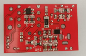
The silk print on the PCB refers to some text and marks on the PCB board. Usually, a color that contrasts significantly with the solder mask oil is used. For example, green solder mask, white silk print , black solder mask, white silk print . Or white solder mask, black silk print and so on. Sometimes other colors are used too, such as yellow or brown. In gerber, a layer called the silk print layer is specially designed, which is also a step of making PCB. The silk print is like a picture on the PCB. It can reflect the position, size and polarity of each component. This is the most basic and important function.
Although the silk print looks simple, there are many important information elements in it. A complete and perfect silk print layer will give a lot of information to the factory and IQC. Because the silk print includes the location and packaging (footprint, polarity) of the components, IQC will use the silk print to compare the components and the pads to help engineers inspect the circuit board and so on. The silk print plays an important role.
As an OEM factory, we are exposed to a wide range of design types and cooperate with engineers in many countries. The PCB boards of different designers in different countries have subtle differences. Today, let’s introduce some of the silk print problems we encountered before and how to improve them.
We have encountered very complicated situations. PCB engineers did not design a good silk print layer. The PCB itself is also due to too many components. To reflect the position number, it must also reflect the package. There is an overlap between the silk print. This makes it difficult to distinguish between the location of the component and the package (package). At this time, pick and place file is needed to confirm the specific components of the location. After we finish the PCB production, before starting the SMT process, the IQC of our factory will first compare each item of the BOM with the real PCB. They mainly check whether each component is attached to the pad. Each pad and mounting hole should have a silk print, which shows the package of each component. This comparison process will prevent many problems from occurring, and is also a guarantee for the smooth progress of subsequent SMT. Usually this process will find and solve many problems.
Under the right circumstances, when the component is placed inside the silk print, it can cover the silk print. Because the package is also called footprint, the size of the components must be the same as the package, indicating that there is no problem with the BOM and the purchased components are also okay. If the component is obviously too large or too small on the silk print of the circuit board, it indicates that the designer has a problem with the design of the circuit board or the selected component. At this time, it is necessary to confirm with the customer and solve the problem in advance to avoid errors after getting on the machine.
In addition, the display component package (footprint), silk print can reflect the polarity of the component. This is very important. Because some components have polarity, designers usually use ± symbols or heavy colors to indicate negative or positive. So when soldering these polar components to the PCB board, you must pay attention to the direction. If the direction is wrong, the PCBA test will not pass, and even the components and boards will be burned out, causing great losses. In order to distinguish the difference, according to the correct component welding direction, the original circuit principle can be realized, and the PCBA can work normally and achieve the designed function.
Silk print can help engineers mark the version, such as V1.1, V1.2, V1.3…
so that they can clearly know which version it is when they receive the product. After many batches of production and many years, each batch can be clearly distinguished, and whether there is a revision can also be seen clearly. The silk print can also be used to record the date or some other information. When a problem occurs, the silk print can be used to trace the time of the problem, the factory and the used components, etc.
The silk print will help engineers to carry out testing and troubleshooting.
The silk print marks the test point or the location of the test program. When a complete PCBA does not work properly, engineers usually check the components one by one. The silk print will make the position of each part clear at a glance, so that the inspection work is not missed.
The PCB board will be marked with prompt words such as high voltage attention, and sometimes the brand and model of the product will be marked on the PCB.
In some cases, in order to reflect the level of PCB and meet the standards, there will be UL silk screen and 94V0 silk print.
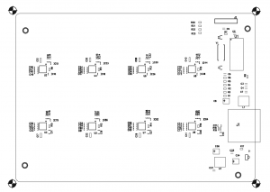
Silk print helps assembly (SMT) work.
When the engineer inspects the gerber, he can judge whether it is single-sided mounting or double-sided mounting by the silk print layer, and judge whether there is a DIP by the drilling layer, whether it is a single-sided DIP or a double-sided DIP. (If there are silk print on both sides of the PCB, it means that it is a double-sided mounting PCB). The silk print helps us to know whether the component should be soldered to the top layer of the PCB or to the bottom layer of the PCB. Generally speaking, the components are soldered on the silk print. Some silk print are like a top view of a component, where some pins should be placed, and the holes of the connector are obvious, which can help the welder to work accurately.
Soldering mask and silk print are the final processes of circuit board prouction, just like putting a beautiful coat on the printed circuit board.
Especially for silk print, high-quality clear silk screen reflects the quality of PCB board to a certain extent. Therefore, when we produce circuit boards, we will use high-grade inks, clean the screen frame, strictly control the intensity of the scraping oil, and control the baking temperature. In this way, the silk print can be clear and high-performance.
https://www.finetechpcba.com/
Our company has more than 40 engineers to solve many gerbers from different countries every day. Some gerber files without a silk print layer are either silk-printed on vias or through holes, or the silk-print is not clear. Our engineers will organize EQ files and solutions. By confirming and modifying with customers, we can solve the problem at the beginning of the project, and make the next step of PCB production and assembly work more smoothly.