SMT is surface mount technology (Surface Mounted Technology) (abbreviation of Surface Mounted Technology), SMT refers to the abbreviation of a series of process processes for processing on a PCB board. PCB (Printed Circuit Board) is a printed circuit board, which is one of the most popular technologies and processes in the electronic assembly industry, which began in 1960.
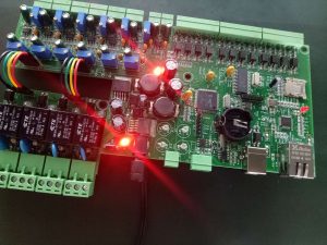
SMT introduction
SMT (abbreviation of Surface Mounted Technology) refers to the abbreviation of a series of process processes for processing on a PCB board. PCB (Printed Circuit Board) is a printed circuit board.
SMT is a surface mount technology (surface mount technology), it is a kind of leadless or short lead surface mount components (referred to as SMC/SMD, Chinese called chip components) mounted on a printed circuit board (Printed Circuit Board, Circuit assembly technology in which the surface of PCB) or the surface of other substrates is soldered and assembled by methods such as reflow soldering or dip soldering.
The electronic products we use around are made of pcb plus various capacitors, resistors, chips, diodes, relays and other electronic components designed according to the designed circuit diagram. Electrical products with different functions require a variety of different smt stickers. Chip processing technology to process.
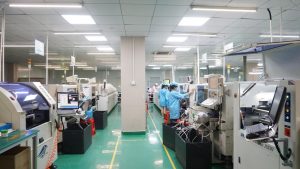
SMT basic process
Solder paste printing --> parts placement --> reflow soldering --> AOI optical inspection --> maintenance --> sub-board.
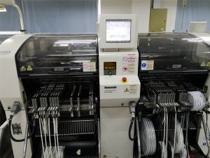
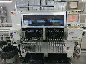
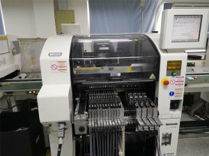
We pursue miniaturization of electronic products, lighter weight, thinner appearance, and the previously used perforated plug-in components can no longer be reduced. Electronic products have more complete functions, and the integrated circuits (ICs) used have no perforated components, especially large-scale, highly integrated ICs, and surface mount components have to be used. With mass production and automation of production, the factory must produce high-quality products at low cost and high output to meet customer needs and strengthen market competitiveness. The development of electronic components, the development of integrated circuits (IC), and the diversified application of semiconductor materials.
The advantages of smt chip processing: high assembly density, small size and light weight of electronic products. The volume and weight of chip components are only about 1/10 of that of traditional plug-in components. Generally, after SMT is adopted, the volume of electronic products is reduced by more than 40%. The weight is reduced by at least 60%. High reliability, high solder joint yield rate. Good high frequency characteristics, reducing electromagnetic and radio frequency interference. More automation, improved production efficiency, greatly reduced costs, and saved materials, energy, equipment, manpower, time, etc.
It is precisely because of the complexity of the process flow of smt patch processing that there have been many smt patch processing factories, specializing in smt patch processing, smt patch processing has made an industry prosperous.
SMT Process
The basic process components of SMT include: stencil screen printing (or dispensing), placement (curing), reflow soldering, cleaning, inspection, and repair
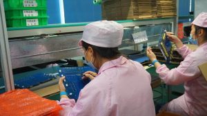
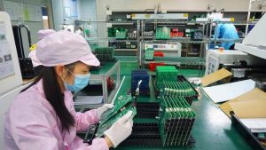
1. Silk screen: Its function is to print solder paste or patch glue on the PCB pads. The tool is usually a steel mesh to prepare for the soldering of components. The equipment used is a screen printing machine (screen printing machine), located at the forefront of the SMT production line.
2. Dispensing: It is to drip glue onto the fixed position of the PCB board, and its main function is to fix the components on the PCB board. The equipment used is a glue dispenser, located at the forefront of the SMT production line or behind the testing equipment.
3. SMT: First, you need to use pick&place files to program component positions and machines. Then use the SMT machine to accurately install the surface mount components on the fixed position of the PCB. The equipment used is a placement machine, located behind the screen printing machine in the SMT production line.
4. Curing: Its function is to melt the patch glue, so that the surface assembly components and the PCB board are firmly bonded together. The equipment used is a curing oven, located behind the placement machine in the SMT production line.
5. Reflow soldering: Its function is to melt the solder paste, so that the surface assembly components and the PCB board are firmly bonded together. The equipment used is a reflow oven, located behind the placement machine in the SMT production line.
6. Cleaning: Its function is to remove the solder residues such as flux that are harmful to the human body on the assembled PCB board. The equipment used is a washing machine, and the location may not be fixed, it may be online or offline.
7. Inspection: Its function is to inspect the welding quality and assembly quality of the assembled PCB board. The equipment used includes magnifying glass, microscope, online tester (ICT), flying probe tester, automatic optical inspection (AOI), X-RAY inspection system, FCT function tester, etc. The location can be configured in a suitable place on the production line according to the needs of the inspection.
8. Rework: Its function is to rework the PCB boards that have failed to detect faults. The tools used are soldering irons, rework stations, etc. Configured at any position in the production line.
SMT classification
PCB SMT is divided into single-sided SMT, double-sided SMT, and SMT+DIP hybrid single side or double side
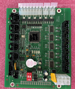
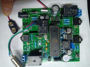
Single-sided assembly
Incoming inspection => silk screen solder paste (point patch glue) => patch => drying (curing) => reflow soldering => cleaning => inspection => repair
Double-sided assembly
A: Incoming inspection => PCB’s A-side silk-screen solder paste (point SMD glue) => SMD PCB’s B-side silk screen solder paste (point SMD glue) => SMD => Drying => Reflow soldering ( It is best to only apply to side B => cleaning => inspection => repair).
B: Incoming inspection => PCB’s A side silk screen solder paste (point patch glue) => SMD => Drying (curing) => A side reflow soldering => Cleaning => Turnover = PCB’s B side point Patch glue => patch => curing => B surface wave soldering => cleaning => inspection => repair)
This process is suitable for reflow soldering on the A side of the PCB and wave soldering on the B side. In the SMD assembled on the B side of the PCB, this process should be used when there are only SOT or SOIC (28) pins or less.
Single-sided SMT+DIP mixed process
Incoming inspection => PCB’s A-side silkscreen solder paste (point patch glue) => SMD => drying (curing) => reflow soldering => cleaning => plug-in => wave soldering => cleaning => inspection = > Rework
Double-sided mixed process
A: Incoming inspection => PCB’s B side point patch glue => SMD => curing => flip board => PCB’s A side plug-in => wave soldering => cleaning => inspection => rework
Paste first and insert later, suitable for situations where there are more SMD components than separate components
B: Incoming inspection => PCB’s A side plug-in (pin bend) => flip board => PCB’s B side patch glue => patch => curing => flip board => wave soldering => cleaning => Inspection => Repair
Insert first, then paste, suitable for the situation where there are more separate components than SMD components
C: Incoming inspection => PCB A side silk screen solder paste => Patch => Drying => Reflow soldering => Plug-in, pin bending => Turnover => PCB side B point patch glue => Patch => curing => flipping => wave soldering => cleaning => inspection => rework A-side mixed assembly, B-side mounting.
D: Incoming inspection => PCB’s B side spot patch glue => SMD => curing => flip board => PCB’s A side silk screen solder paste => patch => A side reflow soldering => plug-in => Wave soldering on side B => cleaning => inspection => rework for mixed mounting on side A and mounting on side B. First paste on both sides of SMD, reflow soldering, then inserting, wave soldering E: Incoming inspection => PCB’s B-side silk screen solder paste (point patch glue) => SMD => drying (curing) => reflow soldering = > Flip board => PCB’s A-side silk screen solder paste => SMD => Drying = Reflow soldering 1 (partial soldering can be used) => Plug-in => Wave soldering 2 (If there are few components, manual soldering can be used) => Cleaning => Inspection => Rework A-side mounting and B-side mixed mounting.
Double-sided SMT+DIP mixed assembly process
A: Incoming inspection, PCB A side silk screen solder paste (point patch glue), patch, drying (curing), A side reflow soldering, cleaning, flipping; PCB B side silk screen solder paste (point patch Glue), patch, drying, reflow soldering (preferably only for side B, cleaning, testing, and repairing)
This process is suitable for picking when large SMDs such as PLCC are attached to both sides of the PCB.
B: Incoming inspection, PCB A side silk screen solder paste (point patch glue), patch, drying (curing), A side reflow soldering, cleaning, flipping; PCB B side point patch glue, patch , Curing, B-side wave soldering, cleaning, inspection, rework) This process is suitable for reflow on the A-side of the PCB.
As an OEM factory, we met many customers’ design materials, and encountered some unreasonable designs, which led to a lot of waste of time and expense. Reasonable design can avoid the failure of PCBA, prolong the service life, and is easy to mount and save costs.
The selection and design of surface mount components is a critical part of the overall product design. The designer determines the electrical performance and functions of the components in the system structure and in the detailed circuit design phase. In the SMT design phase, it should be based on the specific conditions and overall situation of the equipment and process. The design requirements determine the shape of the package and the structure of the surface mount components. Surface mount solder joints are both mechanical connection points and electrical connection points. A sensible choice will have a decisive impact on improving the density, productivity, testability and reliability of the PCB design.
There is no difference in function between surface mount components and plug-in components. The difference is in the packaging of the components. Surface mounted packages must withstand high temperature resistance during soldering. Components and substrates must have corresponding thermal expansion coefficients. These factors must be fully considered in product design.
The main advantages of choosing the right package are:
1) Save PCB area effectively;
2) Provide better electrical performance;
3) Protect the inside of the components from environmental influences such as humidity;
4) Provide good communication links;
5) Helps to dissipate heat and provides convenience for transmission and testing

 PCB assembly/SMT
 PCB Manufacturing
 Components Sourcing
 PCB design