PCB assembly/SMT
 PCB Manufacturing
 Components Sourcing
 PCB design
A few days ago, an American customer asked me, can our factory do a die type IC SMT work? My answer is yes, and our engineers carefully confirmed the specifications and data sheet. There are many technical methods for die type IC SMT soldering. Today, let me introduce what are wafer, chip and die? What is the relationship between them?
1.The meaning of the nouns “wafer”, “chip” and “die” in semiconductors
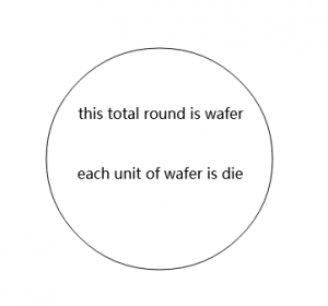
Wafer
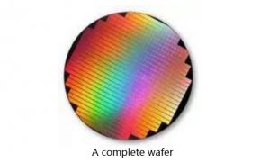
For the look of wafer, we can refer to the picture below. It is round, with specifications of 6 inches, 8 inches, and 12 inches. . . It is made of pure silicon (Si), and the IC wafer chip is produced based on this wafer. Various circuit element structures can be processed on silicon wafers to become integrated circuit products with specific electrical functions.
Chip
The general term for semiconductor components. A wafer with a Nand Flash wafer is first cut and then tested. The intact, stable die with sufficient capacity is removed and packaged to form a Nand Flash chip (chip). The main meaning of a chip is generally used as a carrier, and an integrated circuit is a result produced after many complicated design procedures.
die
A small piece on the Wafer is a wafer body with the scientific name die. After encapsulation, it becomes a particle. A die is a small crystal with an irregular shape that composes a polycrystal, and each crystal grain is sometimes composed of several sub-crystal grains with slightly different orientations. The average diameter of the die is usually in the range of 0.015~0.25mm, and the average diameter of the sub-grain is usually on the order of 0.001mm. A die is a small unit in a silicon chip, including a fully designed single chip and a part of the dicing groove area adjacent to the chip in the horizontal and vertical directions.
2.The connection and difference between the nouns “wafer”, “chip” and “die” in semiconductors
①Differences in material sources
Take the silicon process as an example. Generally, the entire silicon wafer is called a wafer. After the process flow, each unit will be diced and packaged. The die of a single unit before packaging is called die. Chip is a general term for chips, and sometimes specifically refers to packaged chips.
②The difference in quality
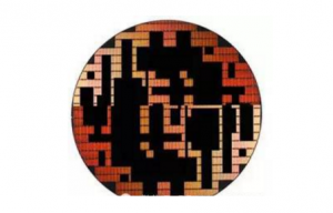
After the qualified die is cut, the original wafer will look like the picture below, just pick the remaining Downgrade Flash Wafer. These residual dies are actually wafers of substandard quality. The removed part, that is, the black part, is a qualified die, which will be packaged into finished NAND particles by the original factory, and the unqualified part, that is, the part left in the picture, will be treated as scrap.
③The difference in size
The die of a single unit before packaging is called die. Chip is a general term for chips, and sometimes specifically refers to packaged chips. Cell is also a unit, but smaller than die cell <die< chip.
Semiconductor refers to a material whose conductivity is between that of a conductor and an insulator at room temperature. Semiconductors are widely used in consumer electronics, communication systems, medical equipment and other fields. For example, a diode is a device made up of semiconductors. Both from the point of view of technology and economic development, the importance of semiconductors is enormous.
Most of today’s electronic products, such as computers, cell phones or digital recorders, have a very close connection with semiconductors. Common semiconductor materials include silicon, germanium, gallium arsenide, etc., and silicon is the most influential in commercial applications among various semiconductor materials.
The semiconductor chip manufacturing process can be divided into raw materials of sand (quartz), silicon ingot, wafer, lithography, etching, ion implantation, metal deposition, metal layers, interconnects, wafer testing and cutting, core packaging , level testing, packaging and so on many steps and each step contains more detailed processes.
Home